


 当前位置:
当前位置:Reference Voltage for Multiple
[11-20 17:32:38] 来源:http://www.88dzw.com 模拟电子技术 阅读:8161次
文章摘要:P-P (approximately 8nVRMS/√ Hz).An array with multiple ADCs may require a reference voltage more accurate than that internal to each converter (the reference internal to MAX144x converters, for example, is ±1% accurate). The following two circuits are submitted as reference designs for such arrays.
Reference Voltage for Multiple,标签:模拟电子技术基础,模拟电子电路,http://www.88dzw.comP-P (approximately 8nVRMS/√ Hz).
An array with multiple ADCs may require a reference voltage more accurate than that internal to each converter (the reference internal to MAX144x converters, for example, is ±1% accurate). The following two circuits are submitted as reference designs for such arrays. They feature a single common low-frequency noise filter, and they achieve high-frequency noise suppression with local decoupling capacitors on individual ADCs.
Single External Reference
Multiple-converter systems based on the MAX144x family are well suited for use with a common reference voltage. The REFIN pin of those converters can be connected directly to an external reference source, eliminating the need for any circuit modification. Moreover, the high input impedance of REFIN (even of multiple REFIN terminals connected in parallel) draws only a small load current.A precision source like the MAX6062 (IC1) generates an external DC level of +2.048V (Figure 1), and exhibits a noise voltage density of 150nV/√Hz. Its output passes through a 1-pole lowpass filter (with 10Hz cutoff frequency) to an op amp (IC2), such as the MAX4250, which buffers the reference before its output is applied to a second 10Hz lowpass filter. IC2 (MAX4250) provides a low offset voltage (for high gain accuracy) and a low noise level. The passive 10Hz filter following the buffer attenuates noise produced in the voltage reference and buffer stages. This filtered noise density, which decreases for higherfrequencies, meets the noise levels specified for precise ADC operation.
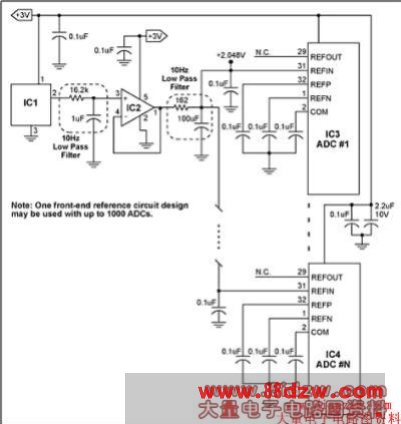
Figure 1. For ultrasound applications, a single low-noise reference circuit drives up to 1000 ADCs.
The converters of the MAX144x family are specified for a typical gain error of ±4.4% (better than ±0.5dB). This performance is better than the gain tolerance of all other building blocks in the signal path of an ultrasound receiver. Note that proper power-up/-down sequencing is ensured because all active parts are driven from the same supply voltage. This approach yields excellent gain matching and a very low noise level with minimal circuitry, and should suffice in many applications that require multiple gain-matched ADCs.
Generating a Precision External Reference
For applications requiring more stringent gain matching (Figure 2), the MAX144x family again is well suited. Connecting each REFIN to analog ground disables the internal reference of each device, allowing the internal reference ladders to be driven directly by a set of external reference sources. These voltages can have an arbitrarily tight tolerance, and the ADCs track them typically within 0.1%. ADCs of this family also feature a 4kΩ resistance across the ladder reference connection, which allows the load to be easily driven even if many ADCs are operated in parallel.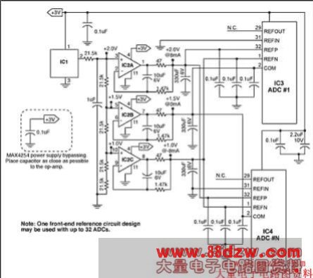
Tag:模拟电子技术,模拟电子技术基础,模拟电子电路,模拟电子技术
《Reference Voltage for Multiple》相关文章
- › Reference Voltage for Multiple
- › Understanding Voltage-Referenc
- › Reference Design for a Class-D
- › 确保打印头电源动态输出电压的参考设计,Reference D
- 在百度中搜索相关文章:Reference Voltage for Multiple
- 在谷歌中搜索相关文章:Reference Voltage for Multiple
- 在soso中搜索相关文章:Reference Voltage for Multiple
- 在搜狗中搜索相关文章:Reference Voltage for Multiple
分类导航
最新更新