


 当前位置:
当前位置:Compact DWDM laser Temperature
[09-13 17:03:11] 来源:http://www.88dzw.com 控制技术 阅读:8666次
文章摘要:By selecting 50kΩ for the input resistance at the inverting pin of the op amp, it follows that the 10uF integrating capacitor must have impedance of at least 50MΩ. Careful selection of components and layout must be applied to guarantee this gain. Taiyo Yuden specifies 1GΩ/µF for capacitors lar
Compact DWDM laser Temperature,标签:计算机控制技术,工厂电气控制技术,http://www.88dzw.comBy selecting 50kΩ for the input resistance at the inverting pin of the op amp, it follows that the 10uF integrating capacitor must have impedance of at least 50MΩ. Careful selection of components and layout must be applied to guarantee this gain. Taiyo Yuden specifies 1GΩ/µF for capacitors larger than 1µF. For a 10µF this equates to 100MΩ. The typical measured values are much higher but without proper layout and assembly techniques, moisture or solder flux can easily nullify efforts to achieve high impedance circuit performance. Testing in an environmental chamber at 0°C can cause water to condense and reduce circuit performance. Leakage currents on the PCB (Printed Circuit Board) can also create problems at this impedance level. It is therefore recommended that a guard ring be placed around the inverting input on the op amp and it's associated components. The location of this guard ring is shown this in Figure 2.
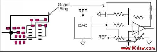
Figure 2. PCB layout for guard ring.
The guard ring functions as follows. Because the DAC output voltage is similar to the op amp's inverting input voltage there is essentially no potential difference between the guard ring and summing junction and its associated components inside the ring. The ring intercepts outside surface leakage currents where they are shunted by the low impedance of the DAC. The low impedance ring protects (or "guards") the high gain summing node from leakage currents. The wider the guard ring trace, the greater effect it will have. A ground plane at the DAC output potential should also be placed on the layer immediately below the sensitive circuit components. Even with the guard ring, water and other surface contaminates can still degrade circuit performance. As a final measure an acrylic based conformal coating should be applied to the cleaned and dried PCB and its components after assembly. PCB assemblers can apply this to the assembled boards if it is specified.
After the op amp generates the error signal, the MAX8520/21 converts the error voltage at the CTLI input to a bipolar output current. The voltage controlled output current of the MAX8520/21 helps to control harmful current surges and provide a programmable current limit. The output current and voltage limits can be independently programmed with external resistors. The MAX8520/21 comes with four power MOSFETs integrated in a small 20 pin QFN package and the ultra small UCSP™ package. Waste heat is expelled through an exposed metal pad on the bottom of the chip, which is then soldered to a copper ground plane on the PCB. The high switching frequency of the MAX8520/21 also helps reduces external component size.
Because of the long thermal time constants exhibit by TEC modules, the control loop must also be slow to maintain stability. The components for the PID loop are selected to provide a 1Hz unity gain crossover. While the DC gain of this loop sets the steady state performance, the AC gain bandwidth of the loop defines the transient response. Achieving the highest stable gain bandwidth will produce the fastest transient response and we know that, with time, the integrator will exponentially reduce the loop error.
Tag:控制技术,计算机控制技术,工厂电气控制技术,控制技术
《Compact DWDM laser Temperature》相关文章
- › Reverse Compatibility of the D
- › Compact DWDM laser Temperature
- › Tensilica设计流程支持Cadence Encounter RTL Compiler工具
- › 英特尔 Parallel Composer入门
- 在百度中搜索相关文章:Compact DWDM laser Temperature
- 在谷歌中搜索相关文章:Compact DWDM laser Temperature
- 在soso中搜索相关文章:Compact DWDM laser Temperature
- 在搜狗中搜索相关文章:Compact DWDM laser Temperature
分类导航
最新更新